
Tekmos Talks Newsletters
A newsletter for the semiconductor industry
Tekmos Talks 2020
|
|
||
| A Newsletter for the Semiconductor Industry | ||
| December 2020 | ||
| Welcome to Tekmos Talks. This month Lynn will talk about Old Design Techniques and Wishes for the upcoming Holidays. | ||
| From the Desk of the President, Lynn Reed | ||
|
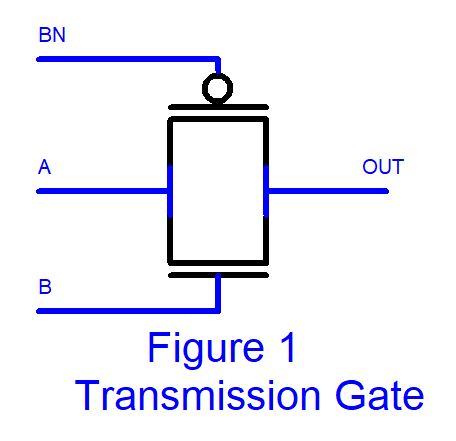
Old Design Techniques Tekmos reverse engineers many older circuits. As we do so, we come across interesting ways to implement logical function that are no longer in common use. I thought that we would show some of them here. Most involve the clever use of a transmission gate. A transmission gate is a basic CMOS switch. It has complimentary enables, and when enabled, allows the input to be connected to the output. The symbol for a transmission gate is shown in Figure 1. There are several things to keep in mind when considering transmission gates. The first is that they are bidirectional. The output is connected to the input through a resistor. This makes a transmission gate very fast, though the presence of the resistance can cause signal attenuation, and ultimately reduces the speed when it drives a large load. The second is that complimentary signals are frequently available in logic design, so they can be used to drive transmission gates without requiring any additional logic.
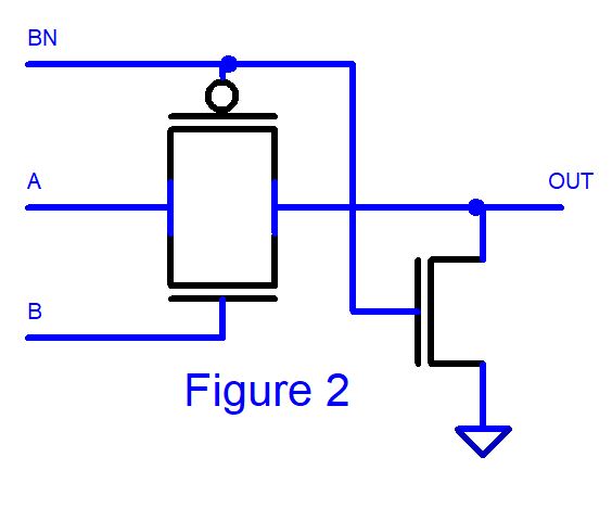
Designers used these transmission gates to save transistors. The cost of transistors has plummeted and are now basically free. But when they were expensive designers went out of their way to avoid using transistors. The function of a transmission gate depends on the surrounding logic. It can be part of a latch, or of another type of gate. This increases the difficulty to understand how it is being used. Gate 1 Figure 2 shows a transmission gate with an n-channel transistor on the output. The gate of the transistor is connected to the enable-bar of the transmission gate. When the transmission gate is not enabled (“B”=0), the output is 0. When it is enabled, the output is the “A” input. This makes it a 2-input AND gate. Currently, it takes 6 transistors to make an AND gate. This uses 3 transistors.
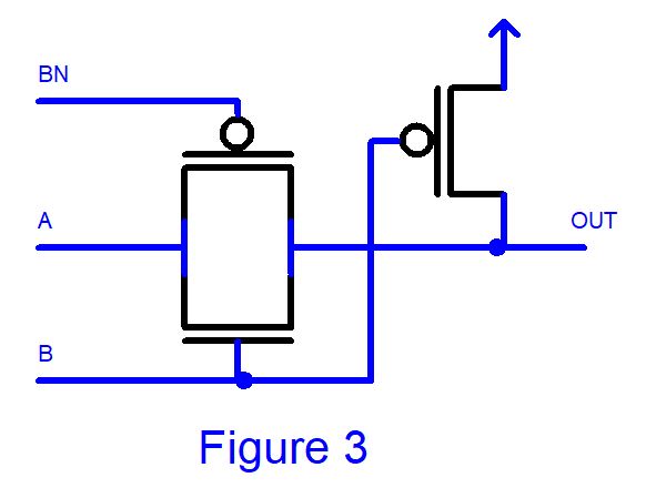
Gate 2 Figure 3 shows a similar gate, but with a p-channel transistor on the output. This creates an OR gate with an inverting “B” input. This can save from 3 to 5 transistors, depending on if an inverter was needed to generate the not B signal.
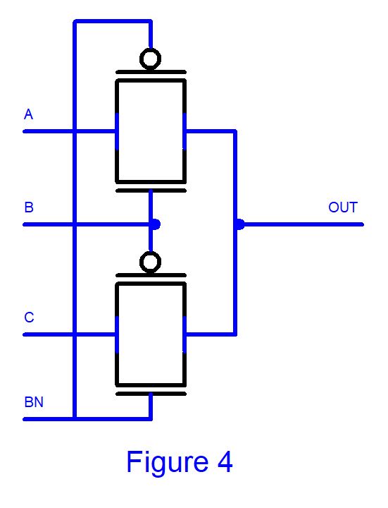
Gates 3, 4, and 5 Two transmission gates can be connected as shown in Figure 4. This can create three different gates, depending on the external signals. The first gate is a 2:1 mux. “B”=1 selects “A” and “B”=0 selects “C” The second and third gates occu
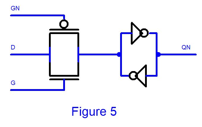
Gate 6 In this gate, shown in Figure 5, the transmission gate drives two cross-coupled inverters. The transmission gate must be stronger than the inverters, which will allow it to overdrive the inverters, producing a latch.
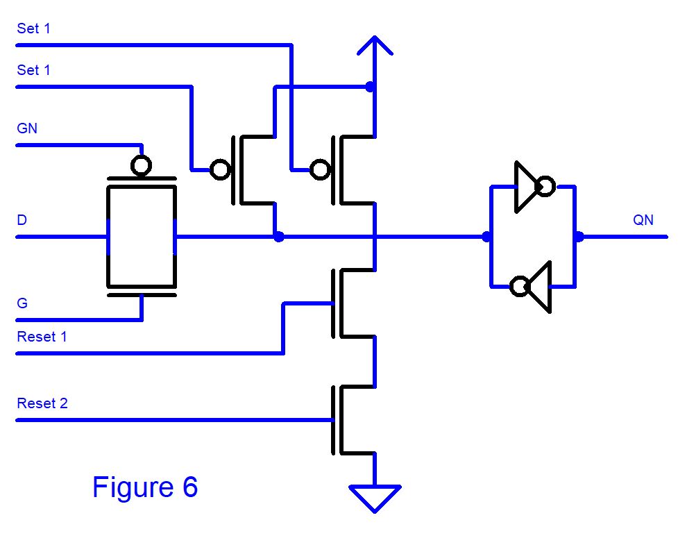
This concept can be extended as shown in Figure 6 with various combinations of P and N transistors producing sets and resets for the latch. In this case, the sets are Or-ed together, while the resets are AND-ed together. Any group of combinational logic can be created either set or reset the latch, provided that the resulting signal is strong enough to overdrive the inverters.
There are other unusual design techniques, which I will cover in a later newsletter.
|
||
| Thank You for Reading Tekmos Talks | ||
|
Thank you for reading Tekmos Talks and helping us celebrate 20 plus years. Sincerely, Lynn Reed, President
|
||
|
|
||
| A Newsletter for the Semiconductor Industry | ||
| November 2020 | ||
| Welcome to Tekmos Talks. This month Lynn will talk about Tekmos' Future Plans and Inside Tekmos; Webmaster to Cad Engineer. | ||
| From the Desk of the President, Lynn Reed | ||
|
Tekmos' Future: Buy vs Lease The Tekmos lease expires this spring. This presents us with a lot of decisions. We have to decide if to move, where to move to, and how much space we need. Well before the Covid pandemic began, we had 20% of our employees working remotely. This has increased to 40% in the current environment. Overall in the company, up to three-quarters of the employees are capable of permanently working at home, with the balance tied to our manufacturing operations. After many internal discussions, we have decided to change our business model to having a distributed company for our professionals instead of us all being in a single location. This decision has a number of interesting consequences which I will cover in future columns. One immediate decision is to determine how much space is required by a dedicated manufacturing facility. The next choice is location. A manufacturing facility does not have the same requirements as a corporate headquarters, particularly since it is rarely visited by customers. So we will be moving manufacturing to the west of Austin, in a low cost and low tax area. This decision was partially motivated by what we see as a deterioration in the business climate within the Austin city limits. That alone could easily be another set of columns. The next choice is rent versus own. Over the years, we have paid a lot in rent. One reason we rented is that we wanted the flexibility to grow by adding space when we added new employees. Now, new employees do not require new space. And manufacturing can easily grow by the addition of additional shifts. So our space requirements are likely to be fixed over the foreseeable future. This makes buying a better deal for us. Another consideration is if the building is a good investment. Is the building likely to increase in value over time? So me made the decision to buy.
|
||
| Inside Tekmos | ||
|
From Webmaster to Cad Engineer, David Abel Earlier in the year Lynn Reed wrote a series of articles detailing Tekmos’ history. One of the common themes throughout Tekmos’ history has been opportunities for growth due to “unique and sometimes unfortunate natural disasters”. One of those disasters was the 2011 Sendai earthquake in Japan. Due to the influx of business from that “unfortunate disaster,” the leadership at Tekmos hired me as an independent contractor to manage and update Tekmos’ website with the purpose of freeing up staff members for more important engineering needs. Nine years later another natural disaster, the novel Corona Virus presented an opportunity for me to join the Tekmos team as a CAD Engineer. Like back in 2011, my hiring as a full time employee at Tekmos was to allow senior engineers to focus on more pressing engineering needs due to various growth opportunities that came our way in 2020 as the world adjusted to Corona. I find it amazing and refreshing how “providence” is again benefiting Tekmos, and now myself.
|
||
| Z.B. Angelich, Director of Marketing | ||
|
Trends in Commercial Property in Texas
Is it better to lease or buy? Buying is a sound option if equity building and resale are important. Can you lower overhead by purchasing? Leasing is a good option if you don't want to commit to upkeep and overhead of a property. One might want to cut down on ongoing property maintenance. A market analysis, financial analysis and other considerations must be addressed. To determine the financial analysis, the present value of the after-tax cost and benefits of owning the property is compared with the after-tax cost of leasing the space. The course of action with the least net cost is the choice of direction. Lease payments, operating expenses, depreciation and interest are deductible expenses, the analysis is usually made on an after-tax basis. The current market analysis of central Texas indicates, with the combination of the ongoing pandemic, people working remote, and a lot of empty buildings, it is a buyers’ market. The region’s average occupancy rate for the highest quality (Class A) office space fell to 88.7% in the April-to-June quarter, down from 90.4% in the second quarter of last year. That’s per the latest figures from Cushman & Wakefield Austin, which tracks the Central Texas office market. As the second quarter approached, COVID-19 had forced the shutdown of most economic activity in March. Until then, Austin’s economy had been one of the nation’s strongest. The economic downturn brought on by the pandemic as well as the influx of homelessness and tent cities, will create property market conditions close to what was seen in the 1980s-real estate crash. Tekmos would be looking at an increased cash flow by taking advantage of low borrowing costs as an owner-occupant, we can deduct interest payments on taxes, we will avoid rent hikes, of which happen annually, including the changing of ownership which can be a challenge. Tekmos is looking ahead to the future in a new work model we have already begun to implement, and to the challenges as well benefits that will arise from this new work paradigm.
|
||
| Thank You for Reading Tekmos Talks | ||
|
Thank you for reading Tekmos Talks and helping us celebrate 20 plus years. Sincerely, Lynn Reed, President
|
||
|
|
||
| A Newsletter for the Semiconductor Industry | ||
| October 2020 | ||
| Welcome to Tekmos Talks. This month Lynn will talk about Dealing with Obsolete Packages & Inside Tekmos' Future Plan. | ||
| From the Desk of the President, Lynn Reed | ||
|
Dealing with Obsolete Packages Tekmos makes replacements for obsolete parts. While we can recreate any old design, our biggest obstacle comes in the packaging of the obsolete parts. In many cases, the packages themselves are obsolete. An example is the BQFP (Bumpered Quad Flat Pack), which was a high pin count package originally developed by AT&T and Intel, and which reached its peak volumes with the Intel 80386SX processor. Today, we are unaware of any vendor that offers this package. Another package that gives us problems are the PLCC packages. The 20 pin is unavailable, and the 28, 68, and 84 pins have very limited availability. A simple solution is to have customers change their PCB to accommodate a new package. But this has problems. Frequently, the demand for older products is driven by regulatory demands. The same regulations that demand the continued use of obsolete parts also require the use of the original PCBs. Changing the board can require a new, expensive, and time consuming qualification. Remaking the original packages also poses problems. Older plastic packages require mechanical tooling to form them into the correct shapes. The three main tools are the book mold, which forms the package, the de-junk tool, which removes extruded plastic from between the leads, and a shear and form tool, which cuts the leads from the lead frame, and bends them into the correct shape. These tools are expensive, costing roughly $100K each. An older package may also require a leadframe, which is generally purchased in 50K minimum quantities. Remaking the package can cost on the order of $350K up front, provided you can locate an assembler willing to do it. Alternatives are needed, and Tekmos offers several. One option is the use of a LGA package. LGA stands for Landed Grid Array, and can be thought of as a BGA type package without the balls. It looks like a PCB with plastic on one side. The parts are formed in a block, and cut apart with a saw, so packages of any size can be made. Tekmos uses this approach to replace smaller PLCC packages. Because the LGA packages are quite thin, they have a maximum size of about 10 mm. Larger packages would tend to warp, and become difficult to attach to the customer’s board. A second option is adapter cards. These come in two varieties. One option is to use a pattern on the bottom of the adapter that matches up with the original package footprint. We then attach our circuit to the top of the adapter. Our circuit must use a smaller package than the adapter, but this is not a problem with current packaging technology. This approach has a difficulty in that the connections are made under the adapter card, and are difficult to inspect. Another option is to use an adapter card with castellated edges. Castellations are a series of plated through holes drilled around the edge of the adapter card. The adapter cards are cut apart directly through the holes, producing the castellated edge. This allows easy inspection of the solder joints. There is an economic disadvantage in that the Tekmos parts can only be attached after the adapter cards are cut apart. This increases the adapter card assembly costs. Each case is different, and Tekmos can work with you to develop the best solution for your needs. Call us for more information.
|
||
| Changes in Latitude & Attitude for Tekmos: Questions to Consider | ||
|
Remote work after COVID-19 Tekmos is thinking seriously about what we want our work paradigm to achieve because of this pandemic. We think we can architect and build systems that will allow us to meet our objectives of an engineering design firm and manufacturer of semiconductors, while maintaining clear and open communication, a key factor in running any company. What do we need to ask ourselves as we look at the future? Our lease will be expiring the 2nd quarter of 2021. We have begun to make decisions about whether we stay in our current location. Where will we move if we do? Do we lease or buy? We have already learned we can save substantially in overhead by moving and creating a new model for Tekmos. What is our overall vision of our ideal work system for Tekmos in the future? Many of our team have worked remote already due to the pandemic. Do we consider adapting a partial virtual model and how does all of this fit together? Executives in traditional industries who spent days and weeks on the road are discovering that a well-managed Zoom meeting can be as effective as a face-to-face — and a lot easier (and less expensive) to organize. While the broad impacts of remote work have yet to be measured across industries and for extended lengths of time, initial studies have found that it can increase productivity and lower employee turnover. (Harvard Business Review) The study, titled “From Immediate Responses to Planning for the Reimagined Workplace,” found that 77% of respondents expect that the number of employees working primarily from home (at least three days a week) will increase postpandemic. Benefits of remote working for both employees and employers: As we move forward in this decision making process we will consider various options about Tekmos’ future manufacturing and engineering facility.
|
||
| Thank You for Reading Tekmos Talks | ||
|
Thank you for reading Tekmos Talks and helping us celebrate 20 plus years. Sincerely, Lynn Reed, President
|
||
|
|
||
| A Newsletter for the Semiconductor Industry | ||
| September 2020 | ||
| Welcome to Tekmos Talks. This month we will share Inside Tekmos Military Lot Qualifications & Program Code Protocol. | ||
| Inside Tekmos | ||
|
Tekmos has had an increase in ASIC products required for military applications. Because of this we have had to incorporate military screening and qualification procedures. Tekmos follows military screening outlined in Mil-STD-883: Test Method 5004.13. This screening consists of tests dedicated to inspect the design, wafer fabrication, and device assembly of a product and is performed on the entire Lot of parts. The tests include Nondestructive Bond Pulls, Temperature Cycling, Electrical Parameter Tests, and more. So far Tekmos has had a 100% success rate on military screening 5004.13.
For Groups B and D, Tekmos sends off parts to an approved test house. These parts, although tested off-site, are constantly being tracked through various communication channels for accurate completion estimates and potential issues needing to be resolved. Once all parts have completed, the test house will send reports and certificates of conformance for the testing performed. The reports are then reviewed by the Production Engineer, Zachary Kolb, and Director of Quality, Kelsey Casto.
Finally, when all testing has been completed the information is collected and compiled together into one report that is sent to the customer. Along with the data, Tekmos provides a First Article Inspection Report using the AS9102 FAI Report Template. Within this report we verify and evaluate all of the tests done and affirm their accountability with sign offs by Zachary Kolb and Kelsey Casto.
|
||
|
Tekmos Program Code Protocol
At Tekmos we offer customers programming of parts for specific orders, applications, and needs from anything such as medical devices, conveyor systems, military parts, consumer technology, to even printers and kilns. It is extremely important from Tekmos’ point of sale that the program code and program related information be accurate for the order when it is received.
Tekmos has implemented a tighter product customer support protocol to meet our customers’ needs during this pandemic. We have done the same with our production check points as they have become more critical during this time before the final shipment to the customer. Customer Support always returns at the back end after delivery to the customer and whenever questions or concerns might develop. We strive to provide the best customer experience always adhering to AS9100D certification.
|
||
| Thank You for Reading Tekmos Talks | ||
|
Thank you for reading Tekmos Talks and helping us celebrate 20 plus years. Sincerely, Lynn Reed, President
|
||
 Unlike the initial screen procedures, the military qualification procedures are outlined in Mil-STD-883: Test Method 5005.17 and only use a small portion of the Lot for testing. Many of the tests are considered destructive, which ultimately means the parts no longer are active for customer use and must be scrapped. Qualification involves 5 groups of testing; Group A: Electrical, Group B: Mechanical and Environmental, Group C: Life Tests, Group D: Package, Group E: RHA (if applicable).
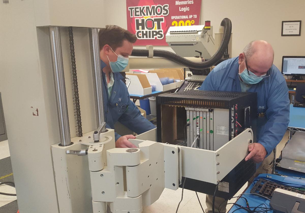 Group A testing is done in-house once production parts arrive from the dedicated assembler. Tekmos begins screening by performing an initial electrical test to remove any assembly rejects from the Lot. After Initial test, parts are then placed in ovens for a burn-in cycle in accordance with TM 1015, for 160 hours at 125ºC. While the parts are under burn-in, Tekmos constantly monitors the current output of the parts to ensure their electrical stability. Once completed, the parts will run through a tri-temperature screening with the same initial test used pre-burn-in. The parts are tested at 125ºC, 25ºC, and -55ºC to make certain the product is meeting the device specifications.
 While Groups B and D are being tested off-site, Tekmos begins the final and longest Group testing in the military qualification, Group C. This testing is in accordance with TM1005, the steady state Life Test. This test is used to demonstrate the reliability of parts under specific conditions over an extended period of time using an oven chamber. The typical conditions used by Tekmos for this Life Test burn-in are; a 125ºC oven, 1000-hour duration, and a sample size of 45 parts. After the 1000 hours, the parts undergo an end-point electrical screening to confirm the parts are still operational post-burn-in.
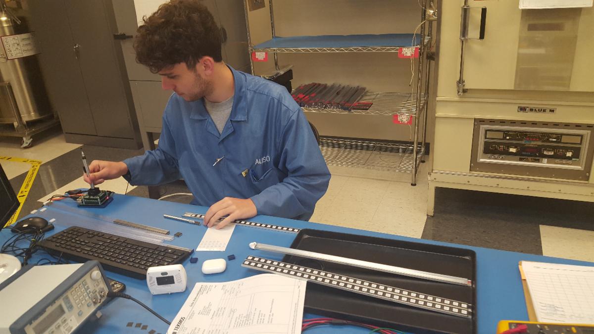 Because automated systems are used regularly by many of us, often not all of the required information for an order is received from the customer. This is where customer service comes in. When the customer places an order for a programmable part we ask for verification of the program file and any related specifics. As part of the order process, Tekmos has created a template to send to customers for all programming code information to be filled out. That could include the hex. file, clock speed, voltage, and other data important to engineers for the parts use. That information is saved in the order file for the customer, our engineering files for the specific customer, and our production team creates a “traveler” that engineers, assembly, our test floor team and shipping can follow so that everything related to the part order including the programming is adhered to. We have one final check with our AP/AR office to verify that all of the order information is correct before it is shipped to the customer.
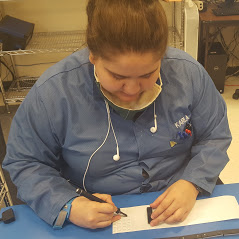 Those currently working remote and communicating the correct information to one another during a more personal and work-related stressful time such as this pandemic, can cause misinformation or no information being passed along in the chain of data. Remote working instead of the office can be filled with distraction and can limit accessibility to work files and data. That is why it is even more important that Tekmos follow stricter guidelines when it comes to programmable parts for our customers.
|
|
||
| A Newsletter for the Semiconductor Industry | ||
| August 2020 | ||
| Welcome to Tekmos Talks. This month Lynn will talk about Tekmos' 900th Design and we will share Inside Tekmos Summer Intern Projects. | ||
| From the Desk of the President, Lynn Reed | ||
|
Tekmos 900th Design As with most semiconductor companies, Tekmos uses an internal number to identify designs. Since we frequently merge multiple designs onto a single layout, we use another number for the layout. And since we may use multiple layouts on a multi-project wafer (MPW), we use a third set on numbers for mask sets.
|
||
| Inside Tekmos | ||
|
Summer Intern Projects
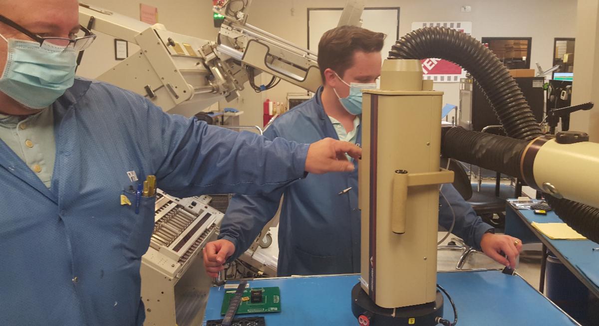
Every company has a combination of both low and high priority projects. The high priority projects are customer driven, and all have deadlines. These are not projects for interns. The low priority projects are another matter. Low priority projects are typically for internal use. There is no specific deadline, and they are usually not manned. And so these are what we assign to the interns. If they succeed, then we have solved a problem. If they don’t, then we are no worse off than we were before. Fortunately, we have had a good deal of success with interns, and have been successful every time. Past projects have included an interface between our tester and our handler that also allowed for a manual start button. Another project involved the use of DSP algorithms for testing a codec circuit. And a third was a test case where we extracted a circuit schematic from a physical layout. This summer, we have had our two interns, Byron Seaberg and Gavin May, working on a dedicated tester for one of our high-volume parts. We have a handler capable of 7 site testing, but we don’t have a tester to go with it. One of our engineers had put together a schematic, but the resulting board had issues. So, we assigned one intern to hardware problems, and the second intern to software problems. The hardware intern identified several wiring issues on the board where 2.5 volt signals were connected to 3.3 volt flash memories. He corrected the schematic, turned the board, and is now debugging it before he returns back to school (MIT). Our software intern has assisted by writing code to exercise the board, and working on USB protocols to interface the tester with a PC. Again, it is a rush to finish before he returns to school (UC Berkley).
|
||
| Thank You for Reading Tekmos Talks | ||
|
Thank you for reading Tekmos Talks and helping us celebrate 20 plus years. Sincerely, Lynn Reed, President
|
||
 This past month we completed our 900th design. As with many of our designs, this 900th design was a reverse engineering of an obsolete part. In this case, the part was a specialty memory consisting of a RAM with a shadow EEPROM that would store and recall the RAM contents with a single write or read. In addition to a small amount of digital logic, this circuit also included a band-gap voltage reference, an internal oscillator with PVT (Process-Voltage-Temperature) control, and multiple high voltage charge pumps. We used an older 0.6u process to obtain 5 volt operation.
 The next question is, when will we reach our 1000th design? That is hard to forecast, but with the recent starting of a set of 7 obsolete 5 volt flash memories and two different obsolete microprocessors, we are about 10% of the way to the next milestone.
 Tekmos makes frequent use of interns, particularly over the summer months. These are college students, majoring in engineering or computing science. The challenge is how to make effective use of a smart, but relatively untrained employee who may only be available for 8 to 10 weeks. Here is how we do it.
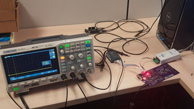
 We try to create jobs that will not only benefit us, but will benefit the interns. The main benefit is doing actual engineering work in an engineering environment. We also try to enhance their experience by letting them participate in engineering design reviews and in manufacturing meetings. This makes the internship a win-win proposition for both of us.
|
|
||
| A Newsletter for the Semiconductor Industry | ||
| July 2020 | ||
| Welcome to Tekmos Talks. This month Lynn will talk about ASIC Design and partnerships, and we will share a 2 part series on Summer Intern Success. | ||
| From the Desk of the President, Lynn Reed | ||
|
ASICs & Design Centers Tekmos is announcing a new program to partner with independent design centers to produce low cost ASICs for use in medical, industrial, and consumer products. This collaboration combines Tekmos’ skills in ASIC design and manufacture with the design centers knowledge of the user applications. This allows Tekmos to develop the ASIC in parallel with the system design, resulting in an overall faster time to market. ASICs provide an alternative to systems utilizing standard products when there are economical, electrical, or mechanical constraints. Economically, ASICs are justified when the manufacturing savings equals the NRE after 6 months of production. This typically occurs for volumes that exceed 250K units per year. ASICs are also justified when there are electrical performance or mechanical restrictions in the application. For example, a biomedical product that must be swallowed has a size constraint that cannot be waived. And some applications require analog measurements that cannot be made with a processors built-in ADC. For these applications, an ASIC is the only solution. Most larger semiconductor manufacturers are driven by manufacturing volume. This leads to minimum sales volume requirements for doing business with them. These requirements result in customers with production volumes between 100k to 5m being unable to take advantage of the benefits of ASICs. This is where the partnership between Tekmos and independent design centers comes into play. At these volume levels, many of these customers utilize independent design centers to create the electrical portions of their end product. Yet many of these design centers may not have made the investment in the design tools necessary to create a successful ASIC. Tekmos has the required ASIC tools and experience. Combining this with the design center’s application knowledge allows for the creation of a cost effective solution for the end customer.
|
||
| Inside Tekmos | ||
|
From the Desk of the Director of Quality, Kelsey Casto
College Intern to Director of Quality-the Tekmos Experience This October will be my 6th year as a Tekmos employee. Oh- how time flies. Tekmos has gotten to see me graduate college, buy my first house, get married, and so much more! So-I think it’s only fitting to write an article about my experience within the company and a few life changing principles I have learned in the many different roles as; Intern, Assembly Engineer, and Director of Quality. I started at Tekmos in 2014 as an Engineering Intern helping the design and layout of Printed Circuit Boards (PCB). I was familiar with working on CAD programs, so I was able to pick up the PCB software easily, but there was one important lesson I still needed to learn; admitting to my mistakes. Not every PCB I designed was functional, which meant my 20 year old self made numerous arguments blaming others for the mistakes. After one failed (expensive) project and my countless excuses blaming others, Lynn Reed, President, sat down in my cubicle with me and shared some wisdom about taking ownership of my work, including the mistakes, because in the end the project is ultimately my responsibility. Those simple, self-explanatory words changed my view on how to embrace mistakes and take ownership. Yes, I still made mistakes on some PCBs, but my attitude towards failure had drastically changed. My next important learning experience came after I got promoted to an Assembly Engineer. This promotion meant I was now transitioning into a role I had little knowledge in and leaving the comfort-ability of PCB designing. I had to embrace getting out of my comfort zone and take initiative on learning a subject outside of the classroom. Although- fellow Tekmos employees graciously helped along the way. Specifically Test Floor Technician, Phil Buck, who spent many patient hours explaining the assembly process of ICs, machine operations/troubleshooting, and even the importance of electrical safety while working on test floors. With his help, I learned how to get comfortable with my new role as an Assembly Engineer and be humble in times of the unfamiliarity. Fast forward one year, VP of Operations, Jon Gehm, introduced me to the Quality Management System (QMS). Initially, I was assisting him with audit prepping and reorganization, but over time he encouraged me to take leadership on the AS9100 quality system upgrade and set a goal to become the Director of Quality at Tekmos. This encouragement really tested my self-confidence and I had to learn to push myself beyond my set boundaries. I had many learning curves on what it meant to be in a Director position, but it eventually led me to grow a voice in meetings, audits, improvement plans, and much more. Eventually I was promoted to Director of Quality and have been at this role since 2017. Because of the leadership and environment at Tekmos I have learned how to admit to mistakes, embrace the uncomfortable, and gain self-confidence. Tekmos offers various internship programs for college students in the summer, as well as openings for design engineer positions for those wanting their own Tekmos Experience.
|
||
| Tekmos Interns | ||
|
Tekmos Engineer Interns Kick Start Careers Tekmos Engineer Intern program provides an opportunity to apply what learning in academic pursuits to real world situations, allowing future engineers to enhance skills, further learning, and gain valuable experience. Our interns are technically excellent Graduates who are looking to forge a career with one of the most successful companies within the field of mixed-signal integrated circuits. Several of our engineers were mentored through our Intern program and currently serve in full time positions including Kelsey Casto, Director of Quality for Tekmos who came to Tekmos as a Junior in college. She has risen up in her 6 years at Tekmos. Clay Abel has worked at Tekmos through high school and breaks from college, and now works as a full-time engineer. This summer we have a new intern in Byron Seaberg and a returning intern in Gavin May. Byron Seaberg learned about Tekmos in high school through Lynn Reed and Jon Gehm, who were both active in Boy Scout Troop 70. Lynn was Byron’s scoutmaster for a period of time and both Lynn and Jon had a large impact on him through the organization. Byron did reach Eagle Scout alongside several other current Tekmos employees Alan Reed, Clay Abel and Adrian De Leon. Byron became interested in engineering through his high school robotics team. He always enjoyed math and science classes during school, and engineering provided a hands-on application of those subjects. Byron is hoping to gain some practical experience with the design and implementation of application specific circuits. He is from Austin, TX. And his hobbies include reading, rock climbing, and board games. Byron graduated in May from Texas A&M University with a major in Mechanical Engineering and minor in Electrical Engineering. He will be pursuing his M.S. in Mechanical Engineering at MIT in the Fall. Gavin May learned about Tekmos through the mentor-ship at his school. Gavin had been mentored by Lynn Reed last summer and returned. Gavin has always enjoyed new things, as well as math and science, so engineering was a clear pathway for him. He hopes to gain real technical experience during his time at Tekmos, and to learn all that he can from the Tekmos Team. Gavin is pursuing a Mechanical Engineering degree from the University of California, Berkeley. He owns a 1966 mustang that has been his restoration project since he was 14 years old. He drives it to work on Fridays. He also plays on Berkeley’s Ultimate Frisbee Team that made nationals this year. Tekmos supports career path development with our Senior Engineers mentoring. We also have a strong history of turning apprentices into successful full-time employees.
|
||
| Thank You for Reading Tekmos Talks | ||
|
Thank you for reading Tekmos Talks and helping us celebrate 20 plus years. Sincerely, Lynn Reed, President
|
||
|
|
||
| A Newsletter for the Semiconductor Industry | ||
| June 2020 | ||
| Welcome to Tekmos Talks! This month Lynn will talk about MOQs, we will learn how Tekmos adapted to some Remote working, and Tekmos extends a thank you. Covid 19 Updates | ||
| From the Desk of the President, Lynn Reed | ||
|
New MOQs on Certain Parts Tekmos makes replacements for many obsolete parts, including processors, memories, and peripherals. We are the solution for replacing parts that have been end-of-life’ed by others. Now, we face end-of-life problems with our own manufacturing of these parts. We retain the ability to manufacture the parts indefinitely. But as with all semiconductors, we must manufacture in discrete lots. Depending on the process technology, and for most of the parts we make, we can reduce the lot size to as few as 3 to 6 wafers. This supports low production volumes. There are times when the volume of an old part drops to very low levels. We have some microprocessors that sell at a rate of 100 parts per year. We don’t mind selling 100 parts from inventory, for as long as we have an inventory. But when the inventory is depleted, we lose the ability to economically support these low volumes. Even with our reduced lot sizes, a wafer lot will produce somewhere between 3,000 and 7,500 parts. So, we build 7500 parts to meet a demand of 100 parts per year? That would leave us with 75 years of inventory, and we simply cannot afford to do that. Instead of discontinuing these parts, we are adopting the following policy. We will continue to sell the following parts with a MOQ of 100 units as long as we have inventory in stock. Once that inventory is gone, then minimum order quantity will increase as noted below.
TK68HC(7)05 Processors
TK68HC05B6 MOQ 3,000,
TK68HC705B16 MOQ 3,000 TK68HC705B32 MOQ 3,000 TK68HC05J1A MOQ 5,000 TK68HC805P18 MOQ 3,000
TK68HC(7)11 Processors
TK68HC11A1 MOQ 3,000 TK68HC11E1 MOQ 3,000 TK68HC11E20 MOQ 3,000 TK68HC11F1 MOQ 3,000 TK68HC11K1 MOQ 3,000 TK68HC711K4 MOQ 3,000 TK68HC711KS2 MOQ 3,000
TK8051 Processors
TK87C451 MOQ 5,000 TK87C749 MOQ 5,000 TK87C750 MOQ 5,000 TK87C751 MOQ 5,000 TK87C752 MOQ 5,000
TK80C186 Processors
TK80C186EC MOQ 3,000
TK80C188EC MOQ 3,000
TK680x0 Processors
TK68020 MOQ 3,000
Flash Memories
TK17LV040 MOQ 3,000
ALL Peripherals MOQ 5,000
TK68HC24 PRU
TK65C51 UART
TK28C94 Quad UART
TK74C3893 Futurebus Driver
TK74FCT280TQ Parity Generator
|
||
| Inside Tekmos | ||
|
Tekmos in a COVID-19 world, by Alan Reed Overnight the world changed when across the globe places started to shut down due to COVID-19. Companies went from a central workspace to a remote workplace, providing a unique new set of problems. Tekmos has strived to provide a smooth transition in these times. Leading up to the work from home orders, we took precautions to prepare everyone the option to remotely work. At the time Tekmos had an asymmetric network connection, meaning that the down and up speeds weren’t the same; in our case as with most asymmetric connections, the down speed was much faster than the up speed. Normally this is fine and you don’t really bat an eye about, but when you switch your business model from being in a centralized location to having everyone remote and access the central resources at the same time, it becomes a big problem The real puzzle is how do you get everyone talking to the resources at the same time without clogging your already limited network bandwidth. The solution was in theory relatively easy, but in practice more difficult than it would seem. You limited people’s need to access networked information. We moved a lot of the files into our repository then had people check out a local copy of them and submit it back when they were done or had updated them, much like the way a library works. This freed up bandwidth and allowed users to work from home remotely without hogging all of our bandwidth. The next problem was training the users to switch over to the remote mindset. This required training on several new programs needed to access our network and connect to servers. By the time this was all done and implemented, Austin had issued its Work from Home order, and we as a company were prepared for it.
|
||
| Tekmos Thanks | ||
|
Tekmos Thanks Our Customers, Suppliers & Vendors June 1, 2020 To our valued customers, suppliers and vendors,
Tekmos would like to extend our gratitude to you for your continued valued support in keeping us fully operational as an essential business that is part of the critical infrastructure of the United States and around the world during the Covid-19 pandemic.
The products we deliver to the consumer, medical, industrial, aerospace, military, and high temperature industries have become even more important.
We extend our sincerest thanks to all Tekmos customers, suppliers and vendors for your ongoing commitment to us during these unprecedented times.
As we move ahead to better times, we look forward to the new challenges and successes they will bring.
Sincerely,
Lynn Reed
President, Tekmos
|
||
| Thank You for Reading Tekmos Talks | ||
|
Thank you for reading Tekmos Talks and helping us celebrate 20 plus years. Sincerely, Lynn Reed, President
|
||
|
|
||
| A Newsletter for the Semiconductor Industry | ||
| May 2020 | ||
| Welcome to Tekmos Talks! This month Lynn will talk about Guard Banding, we will hear from Director of Quality, Kelsey Casto on Quality Metrics and we will visit Inside Tekmos Customer Support. Covid 19 Updates | ||
| From the Desk of the President, Lynn Reed | ||
|
Guard Banding The semiconductor manufacturing process is not perfect, and produces a percentage of defective parts. So, all parts are tested to ensure that they operate correctly and meet specifications. Testing the parts is expensive, and particularly so when the parts are tested over the specified temperature ranges. Testing parts at the high temperature is straight forward, requiring a handler with a heater. Cold testing is more difficult, because ice tends to form around the test socket, creating a mechanical obstruction that prevents further testing. It is common to see testers stopped, with test technicians using hair dryers to melt the ice. There must be a better way, and there is. And it is called guard banding. Device parameters change with voltage and temperature according to the laws of physics. Parts get faster and stronger with higher voltages and lower temperatures. And they get slower and weaker with lower voltages and higher temperatures. Knowing this, we can pick a voltage for room temperature testing that causes the device parameters to behave the same as if we were using the specified voltage at an temperature extreme. We call this guard banding. While the theory sounds easy, real life requires more work. The question is where to set the limits. Most critical specifications involve maximum timing specifications, which corresponds to minimum voltage and maximum temperature. The first step is to measure the part performance at both room and elevated temperature at the minimum voltage, and determine how much the timing parameters change. One option is to tighten up the timing measurement to reflect this shift. If a part has a specification of 50 ns, and shifts 5 ns with temperature, then it can be tested at 45 ns at room temperature to guarantee the temperature performance. A second option is to lower the supply voltage until the delay has shifted by 5 ns. This new voltage can be used to test the part at the 50 ns specification. And a third option is to use a combination of reduced voltage and tightened timing. Every part is different, and may contain analog components or design techniques that restrict the voltage ranges of the part. It falls to Product Engineering to select the best approach for guard banding. Guard banding can also be used to improve manufacturing yields. A part may go through multiple tests during its manufacture. There can be a probe test, a second probe test if the part contains flash, a final test, and occasionally temperature tests. If a part is at the very edge of a specification, it might fail a later test after it has accumulated more manufacturing cost. To prevent this, tighter voltage limits can be used at the earlier tests to fail these parts, resulting in higher manufacturing yields at the later steps. Guard banding is one of the many techniques that Tekmos uses to provide high quality parts at reasonable costs to our customers.
|
||
| Support | ||
|
From the Desk of the Director of Quality, Kelsey Casto
Beneficial Quality Metrics Although Quality Metrics sound uninteresting to the standard employee, any Quality representative should know that those metrics are the unsung heroes of a healthy company. Quality Metrics are also known as Key Performance Indicators (KPI's), which measures the success of a company based on meeting specific goals and targets set by Management. Tracking KPI’s play a vital role in properly determining if a department is functioning correctly. Unlike a person’s relative opinion on a department’s status, i.e. “I think the Sales Department has been doing well this quarter”, Quality Metrics use a numerical value to assess the department, along with creating a target goal, i.e. “The Sales Department sent out 72 quotes this quarter, which surpassed the target goal of 60 quotes.” These numerical values help management evaluate the department quickly and bypass the possibility of a biased opinion. Metrics also help determine trends occurring in the company. In the above example, if the Sales Department continues to surpass the target goal every quarter, this may be an indication to management that it is time to raise expectations. This could include, allowing more throughput on a production floor, incorporating additional capabilities, or taking on more projects. Of course, if metrics start to trend negatively, management will then have to discuss action plans to get the department healthy again. Implementing action plans first consist of asking the questions; What will be done to get back on track, What resources are required, Who is responsible for the new implementation, and When will the implementation be completed. These questions will initiate movement and gear people back towards success. Tekmos has Quality Metrics in all core departments. Here are a just few; Average Response Time for Sales Inquires, Number of Supplier Late Deliveries, Raw Stock Cycle time to Finished Goods, and more. Tekmos’ metrics were chosen with the help of our President, VP of Operations, and myself – Director of Quality. Each of us brought different experience and understanding of the Organization to accurately assess what a “healthy” Tekmos should look like. Tekmos’ Metric Practices;
|
||
| Inside Tekmos Customer Support | ||
|
Customer Support During Natural Disaster Tekmos has set in place proactive measures and action plans to address global pandemics and disasters for our customers and vendors around the world, and of course our dedicated employees. We understand that many of our customers continue to operate like us, or are looking to reopen operations. Tekmos is deemed part of the “critical infrastructure” designation by the U.S. Department of Homeland Security, and we have continued to remain operational. Here at Tekmos our customers come first. We build sustainable relationships of trust through open and interactive communication responding to a customer request within a 24-hour period, often within 1 hour. Customer Support assists with placement of orders from the date of entry, follow up with changes of shipping dates, push outs, pull ins and Return Merchandise Authorization or RMA’s for parts still under warranty. At Tekmos we pride ourselves on excellent customer support, but occasionally there may arise a concern with a customer. When that happens we resolve product or service problems by clarifying the customer's complaint; determining the cause of the problem; selecting and explaining the best solution to solve the problem; expediting correction or adjustment, and following up to ensure resolution. We have to have good product knowledge of the 700 parts Tekmos carries, market knowledge of what customers are looking for, great listening skills, and ability to resolve issues into solutions. During the past few months all of us have experienced a new way of looking at things, how we interact and do business and live our everyday lives. Chaos theory states that the things that change the world are tiny things, even a virus. Tekmos is here for our customers and we want to thank all of you for your patience and support of Tekmos products yesterday, today and tomorrow. Zeta Angelich, Customer Support/Marketing
|
||
| Thank You for Reading Tekmos Talks | ||
|
Thank you for reading Tekmos Talks and helping us celebrate 20 plus years. Sincerely, Lynn Reed, President
|
||
|
|
||
| A Newsletter for the Semiconductor Industry | ||
| April 2020 | ||
| Welcome to Tekmos Talks! This month Lynn will expand on Tekmos' History, we will hear from webmaster Dave Abel Inside Tekmos and we have an updated Covid-19 Statement. | ||
| From the Desk of the President, Lynn Reed | ||
|
Tekmos History, Part 2 2011 – Sendai Earthquake Tekmos had reverse engineered the 6805 and 6811 CPU cores, and was offering a few processors as replacements for obsolete Freescale / Motorola parts. Freescale had already decided to End-of-Life most of the processors in these product lines. All of these parts were made by a Freescale fab located in Sendai, Japan. On March 11th, 2011, a magnitude 9 earthquake struck Sendai, and destroyed the Freescale fab. In response, Tekmos developed a special gate array that contained EEPROM and an 8-bit ADC. We used that array to produce a large number of different clones of the Freescale processors. This included the 6805 B, C, J and L series, and the 6811 A, D, E, F, K, KA, and KS series. We also made a replacement for the 68020 processor. 2013 – The Fracking Boom, and Bust The fracking boom greatly increased the demand for high temperature circuits. Back in the days of vertical oil drilling, there was minimal demand for downhole electronics. Fracking, with the horizontal drilling, changed that, as electronics were required to steer the drilling bit. Horizontal drilling also can require drilling through extra hot zones to reach relatively lower temperature areas that contain oil. In response to this demand, Tekmos developed an ASIC technology based on a SOI process that operates up to 300ºC. We also pushed some of our processors made on bulk silicon up to the 175-200ºC range. Fracking was very successful, and returned America back into the world’s largest oil producer. Unfortunately, that caused a glut of oil, which has greatly reduced the demand for high temperature electronics. Boom and bust is a characteristic of the oil market. 2017 – Rebuilding the Military For a number of years, the US military budget did not support maintenance, and as a result, required replacement parts were obtained from other airplanes. After 8 years, a large number of military aircrafts were grounded for a lack of parts. That changed in 2017, and the military was again able to buy replacement parts. However, in those 8 years, a number of parts have become obsolete, and were no longer available. Tekmos received a number of contracts for the replacement of some of these obsolete parts. These contracts also caused Tekmos to develop a full military lot qualification capability. 2018 – Into Consumer Products Tekmos had an opportunity to replace a consumer product ASIC whose supply chain had been disrupted. In order to achieve sub $0.50 pricing, Tekmos made technical advancements in a number of areas. We advanced to using a 180 nm technology to cut the die costs. We started using QFN packages to minimize the assembly costs. And we have invested in new testers, multi site testing handlers and advanced tape and reel equipment to cut back-end costs. This has left us well positioned for this market. 2020 – Covid-19 We now find ourselves in the midst of a new crisis, and it is not clear how this will develop. With each crisis, there is opportunity. We believe that this crisis will result in demand of more diverse and robust supply chains, which will increase the opportunity for second sourced ASICs. And we plan to play a role in that.
|
||
| Inside Tekmos | ||
|
Inside Tekmos with Webmaster, David Abel
Tekmos New Website Last year during one of our weekly marketing meetings we decided that it was time to upgrade our website to better enhance Tekmos’ products and services. With the help of Randy Reed and Zeta Angelich, and approval of Lynn Reed, we chose a template that utilized advancements in web design featuring Drag & Drop Layout and Page Builder. Randy of REEDESIGN created all new graphics for the site while Zeta updated the Text Headings and accompanying Text Blocks. One newly added feature to our Home Page is Tekmos Market Segments. We conveniently added linkable buttons to the following markets that Tekmos specializes in: Consumer, Medical, Industrial, Aerospace, Military, and High Temperature Markets. We also added linkable buttons to our Solutions, Products, and Support pages. Each of these links enables our customers to navigate the site in an orderly fashion. Additionally, there is now a simple contact form at the bottom of every page for easy communication. In the Main Menu customers can learn about Tekmos by hovering over the About or Contact tabs and selecting pages from the corresponding drop-down menu. Customers can also hover over the Products tab in the Main Menu and a mega menu conveniently displays Tekmos’ products in four separate categories: Microprocessors, Flash Memory, High Temperature Semiconductors, and ASICs. Returning customers frequently come to our site to read Tekmos Talks Newsletters and Tekmos’ Blog. Both of those can now be found under the About tab drop down menu. All in all we here at Tekmos hope our customers find the new site design refreshing and easy to follow.
|
||
| Support | ||
|
Tekmos Updated Covid-19 Statement Here at Tekmos we have taken proactive measures and action plans to address COVID-19 for our employees, customers and vendors around the world. We would like to reassure “the internal supply chain for Tekmos continues to flow and we do not anticipate a supply chain disruption because of this pandemic.” Tekmos is considered an Essential Business and will follow all city policies related to being an Essential Business. Tekmos shall:
· Continue operations and watch for signs of disturbance in our supply chain and/or future business flows caused by COVID-19.
· Allow employees to work from home, unless needed for specific operation tasks onsite.
· Create alternate work plans for employees choosing to work from home. This includes, but is not limited to, upgrading internet bandwidth to better accommodate telecommuting, installing TeamViewer, Open VPN, and GoToMeeting on computers for accessibility to normal Tekmos operations.
We will continue “business as usual” and will meet the needs of our customers while maintaining Center of Disease Control (CDC) and our state and federal government direction and measures. Please do not hesitate to contact Tekmos for any concerns or questions as we all work toward a speedy recovery to the nation and world. Lynn Reed, President Tekmos
|
||
| Thank You for Reading Tekmos Talks | ||
|
Thank you for reading Tekmos Talks and helping us celebrate 20 plus years. Sincerely, Lynn Reed, President
|
||
|
|
||
| A Newsletter for the Semiconductor Industry | ||
| March 2020 | ||
| Welcome to Tekmos Talks! This month Lynn will talk about Tekmos Supply Chain and we will hear from Director of Quality, Kelsey Casto about Qualification Testing. | ||
| From the Desk of the President, Lynn Reed | ||
|
Tekmos Supply Chain Not Affected by Corona Virus Much is being said in the news about the spread of Corona Virus (COVID-19). As the leader and President of Tekmos, I would like to reassure our customers by stating that “the internal supply chain for Tekmos does not go through China. Tekmos has received inquiries from customers. While we have several partners located in Asia, none of Tekmos product is manufactured in the People’s Republic of China. As a result, we do not anticipate any supply chain disruption as a consequence of the outbreak of the virus.” The outbreak of corona virus disease (COVID-19) was first reported from global economic hub, Wuhan, China, December 31, 2019. The US Center for Disease Control (CDC) and The World Health Organization (WHO) are working closely with global experts, governments and partners to rapidly expand scientific knowledge on this 40 year old virus and to slow the spread of this outbreak. Corona virus represents the name of a number of different viruses that infect humans, other mammals and birds. Typically, in humans it causes a mild respiratory infection resembling a cold. The infamous SARS virus is a corona virus. It gets its name from its appearance in electron microscopy where it has a fringe or halo surrounding the viral body. (see photo) The latest outbreak in China is of a strain called COVID-19 or SARS-CoV-2. It is characterized by a high morbidity (high infectious rate) but low mortality. There is no vaccines or antiviral drugs to treat corona virus infection, but it is susceptible to desiccation, heat and detergents like most enveloped viruses. (D.R. Schneider, PhD). Tekmos did experience some slow down due to the Chinese New Year celebrated in many areas of Asia, during the start of 2020. Tekmos wants our buyers and distributors to be aware that all is going “business as usual for Tekmos and our customers.”
|
||
| Tekmos Events | ||
|
Tekmos Upcoming Events Tekmos will once again sponsor HiTEC 2020 International Conference and Exhibition on High Temperature Electronics. Tekmos considers the advantage of exhibiting at a conference in that it provides feedback about what customers really want to see in products. The event will take place April 28-April 30, 2020 in Albuquerque, New Mexico at the Marriott Pyramid North. This annual conference, alternates venues between the U.S. and England, and is dedicated to high temperature electronics, ranging from the relatively cool 175ºC up to the 1200ºC range for Silicon Carbide. It also covers high temperature materials and passive components. HiTEC 2020 is a leading biennial conference dedicated to the advancement and sharing of knowledge of the high temperature electronics industry. HiTEC 2020 will be the forum for presenting leading high temperature electronics research results and application requirements. It will also be an opportunity to network with colleagues from around the world working to advance high temperature electronics. The event will also combine other conferences on thermal and power packaging and CICMT.
|
||
| Support | ||
|
From the Desk of the Director of Quality, Kelsey Casto
Tekmos uses two generic qualification standards; MIL-STD-883 and JESD47. Both of these standards have compliance testing for the device’s Electrical Capability, Environmental Strains, Life Potential, and Package Assembly Integrity. These tests allow the device to be looked at from all angles and predict whether the device can survive under typical stresses seen in the semiconductor industry. However, some testing is dependent on the final application of the device. If the final application is prone to jolt movements but rarely exposed to alternating extreme temperatures, then a focus on the Package Assembly Integrity testing; I.E. Bond Pull Strength, Bond Shear, and Die Shear, might be more beneficial than the Environmental Strains; I.E. Temperature Cycling. Another testing dependent could be from a Product Change Notice (PCN). If a PCN is sent due to a Wafer Design Change, then it would be more useful to perform Electrical Capability testing rather than Package Assembly Integrity. Of course, if any time a customer desires a full qualification, then Tekmos will be happy to accommodate. Incorporating these qualification tests has come with learning curves and challenges. One main challenge was our project management process had to be revamped to keep up with the additional testing. Majority of the qualification tests are performed by outside suppliers, which means there needs to be extra precaution on lead-time agreements, material management, cost evaluations, and final review of reports. As the Director of Quality, I have taken these new additions to project management as my responsibility. Within the last few months, I have been beta testing a new tool that captures all steps in the qualification process, as well as tracks lead-times and cost trends. Tekmos is hoping this implementation will reduce human error risks, and accurately assess upcoming qualifications. A key player in our Qualification Testing has been our Product Engineer, Zachary Kolb. He was hired back in April of 2019 and has been the main person involved in First Article Inspections. Along with receiving my many pestering, if not annoying emails and phone calls, he is the mastermind behind the qualification tests performed at Tekmos. He is responsible for coordinating information and material with our suppliers, setup and testing of inhouse qualifications, and report generating. He has been a great asset to Tekmos and continues to help maintain structure and organization in device qualifications. If you have any questions involving our First Article Inspection Qualifications, please feel free to email me at; kelsey.casto@tekmos.com Zachary Kolb verifies a Life Test Burn-in Board before entry in Tekmos’ calibrated oven.
|
||
| Thank You for Reading Tekmos Talks | ||
|
Thank you for reading Tekmos Talks and helping us celebrate 20 plus years. Sincerely, Lynn Reed, President
|
||
|
|
||
| A Newsletter for the Semiconductor Industry | ||
| February 2020 | ||
| Welcome to Tekmos Talks! This month Lynn will talk about plans to streamline sample ordering and small quantities from our website. Inside Tekmos we introduce our Test Floor Manager. | ||
| From the Desk of the President, Lynn Reed | ||
|
Tekmos to Streamline Sample Ordering Tekmos is streamlining sample ordering with our website online form inquiries. Our marketing team has begun the process to place Tekmos standard parts in an online inquiry system that customers will be able to purchase samples of parts to qualify for their systems, and request quantities of 100 parts for smaller orders. We will start with the 80C51 microprocessor family and will add the Flash Memory parts upon completion of the data base creation for the 80C51 microprocessors. The price for each part will be visible to customers that visit our website. There will be an “Order Now” icon that a customer can go to, find the part they are looking for, advise whether the purchase is for samples, or if already qualified, and purchase a quantity of 100 by filling in the form that will be sent to Tekmos Customer Service Department at orders@tekmos.com. We have decided to do this to make it easier for our customers to order samples as well as for customers who require a smaller quantity. Larger quantity purchases are available through our distributors and sales reps, and at the sales@tekmos.com link provided on our website. Members of our sales team always respond to customers within a 24 hour period to provide a quote and to assist with purchases.
|
||
| Tekmos Events | ||
|
Tekmos Upcoming Events Tekmos will once again sponsor HiTEC 2020 International Conference and Exhibition on High Temperature Electronics. Tekmos considers the advantage of exhibiting at a conference in that it provides feedback about what customers really want to see in products. The event will take place April 28-April 30, 2020 in Albuquerque, New Mexico at the Marriott Pyramid North. This annual conference, alternates venues between the U.S. and England, and is dedicated to high temperature electronics, ranging from the relatively cool 175ºC up to the 1200ºC range for Silicon Carbide. It also covers high temperature materials and passive components. HiTEC 2020 is a leading biennial conference dedicated to the advancement and sharing of knowledge of the high temperature electronics industry. HiTEC 2020 will be the forum for presenting leading high temperature electronics research results and application requirements. It will also be an opportunity to network with colleagues from around the world working to advance high temperature electronics. The event will also combine other conferences on thermal and power packaging and CICMT.
|
||
| Inside Tekmos | ||
|
Inside Tekmos: Test Floor Production Manager
2020 is his 6th year at Tekmos. Adrian was sought out by the Vice President of Operations after meeting at one of the elite trainings the Boy Scouts of America has to offer, the Wood Badge. Adrian is an Eagle Scout, the highest rank in Boy Scouts of America, a distinction that several Tekmos Team members hold including President Lynn Reed. Adrian has also earned every merit badge, an accomplishment in itself. Only 4% of Boy Scouts have achieved this rank since its inception in 1911. Some of the priorities of the test floor include: Managing and ensuring safe, quality test floor operations for the testing and programming of various semiconductors, microcontrollers and microchips. Other priorities include the enforcement and maintenance of quality control and environmental industry-respected best practices to meet customer, and applicable regulatory requirements. Tekmos uses several types of machines needed in Fabless facilities, such as hot and cold temperature forcing probes, bake ovens, gravity-fed MCTs, an automatic multitester, a pick-and-place Aetrium, V-Tek Tape & Reel machines, and the newest machine, the Exatron pick-and-place handler. Tekmos uses ATEs to reduce manufacturing costs, improve yield, and specifically to prevent defective devices ending up with consumers. Tape and reel equipment as the name implies, is the equipment used in packing and sealing finished products into individual pockets of a carrier tape, and in rolling this tape onto a reel. Tekmos uses tape and reel when a customer requires it as well as for large quantity part orders. Taping and reeling is an alternative packaging process for small surface mount devices that are impractical to ship in tubes. Tekmos ships parts in tubes, tape and reel and other packaging when required. An average day will consist of receiving new orders and systematically organizing it into the test floor process flow. At the same time machines are continued running processing chips and completed orders are prepared for outbound shipments. Meeting customer ship dates is a daily process that the test floor strives to achieve. Adrian takes great pride in his management of Tekmos' Test floor. He holds a BA in Business Administration from St. Edward’s University in Austin, Texas.
|
||
| Thank You for Reading Tekmos Talks | ||
|
Thank you for reading Tekmos Talks and helping us celebrate 20 plus years. Sincerely, Lynn Reed, President
|
||
 Adrian DeLeon is the Post Manufacturing Test Floor Manager for Tekmos, a highly focused, and challenging leadership position in an often-fast paced environment. He is accountable for managing communications with test floor crew, production, customer service, and operations of schedules and systems that guarantee inventory control, finished goods, shipping of products, and an overall effective and efficient production flow.
|
|
|||
| A Newsletter for the Semiconductor Industry | |||
| January 2020 | |||
| Welcome to Tekmos Talks and Happy New Year! This month Lynn talks about the year in review and a history timeline of Tekmos, and we will share Inside Tekmos holiday events. | |||
| From the Desk of the President, Lynn Reed | |||
|
Tekmos History; Planned & Providence I have been wanting to put together a history timeline of Tekmos and share the unique and sometimes unfortunate natural disasters that have helped shape and grow our company to produce custom integrated circuits, solutions ranging from high volume cost reductions for existing applications, drop in replacements for obsolete parts, and creating entirely new products. Our markets have also expanded as we have evolved with planning and fate, opening doors to Consumer Electronics, Aerospace, Military, Industrial, and Medical. We have become leaders in the industry of custom analog and mixed-signal Integrated Circuit (IC) solutions with over 900 designs. 1997 – Founded Tekmos was founded as a spin-off of Flextronics Semiconductor. We started off as a pure design center, doing contract design on a number of projects. The designs ranged from small FPGA conversions for ASIC providers to large FPGA-based systems for on-demand cable companies. 1999 – First Proprietary Chip We heard of a case where Motorola needed a replacement of a part they had once made in order to satisfy one of their major companies. The part was a 68HC24 Port Replacement Unit. We offered to make it for Motorola, and they accepted. As part of the deal, they agreed to forward inquiries for this part to us. Overnight, we acquired several hundred small customers, and a part with a collective volume of over 100K per year. This changed our thinking, and we switched from being an independent design center into a fabless semiconductor company. 2000 – The Dot-Com Crash and Lucent The dot-com crash started in 1999 and lasted for several years. The contract design market collapsed, which made us glad we had switched to selling chips. At the same time, the semiconductor division of ATT was spun off as Agere. In a cost cutting move, Agere end-of-life’ed most of the chips used by Lucent in the telephone switches. Many ASICs were put out to bid, and Tekmos was successful in winning many of them. This started our involvement in the Telecom industry. We also were able to recreate several obsolete chips that became standard products. One of these was the TK17LV040 serial memory. This was our first stacked die product, which we have since used in many different products. 2005 – Katrina Katrina struck Louisiana in August of 2005. Katrina destroyed a number of local exchanges in New Orleans. These centers used a custom chip that consolidated a number of phone lines into a 40 MHz link to the main office. Tekmos started a rush program to recreate the chip and provide the 60K units necessary to restore phone service to New Orleans. This was our first rush order, and we developed capabilities that we continue to use today. Next month I will fill in the blanks with more stories and history about Tekmos.
|
|||
| Tekmos Events | |||
|
Tekmos Attends Consumer Electronics Show Tekmos President, Lynn Reed and Vice President of Business Development, Bob Abrams will be traveling to the Consumer Electronics Show (CES) in Las Vegas January 7-10. It is the world’s largest consumer technology show with over 175,000 attendees, over 300 sessions on various topics related to technology, and 4,500 companies exhibiting their newest innovations. The keynote speaker this year is Ivanka Trump. Tekmos Attends and Will Sponsor HiTEC 2020 Tekmos will once again sponsor HiTEC 2020 International Conference and Exhibition on High Temperature Electronics. Tekmos considers the advantage of exhibiting at a conference in that it provides feedback about what customers really want to see in products. The event will take place April 28-April 30, 2020 in Albuquerque, New Mexico at the Marriott Pyramid North. This annual conference, alternates venues between the U.S. and England, and is dedicated to high temperature electronics, ranging from the relatively cool 175ºC up to the 1200ºC range for Silicon Carbide. It also covers high temperature materials and passive components. HiTEC 2020 is a leading biennial conference dedicated to the advancement and sharing of knowledge of the high temperature electronics industry. HiTEC 2020 will be the forum for presenting leading high temperature electronics research results and application requirements. It will also be an opportunity to network with colleagues from around the world working to advance high temperature electronics. The event will also combine other conferences on thermal and power packaging and CICMT.
|
|||
| Inside Tekmos | |||
|
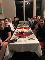
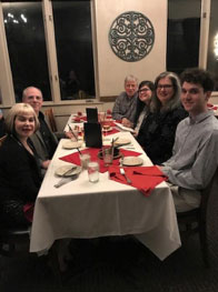
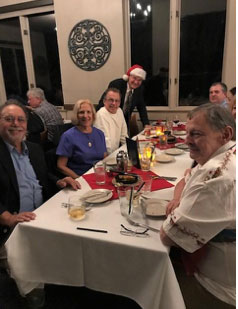
Tekmos Celebrates the Holidays at Z Tejas
Tekmos Team members gather together for most major holidays to celebrate, spend time together off the job, and relax a little. This year’s Christmas/Holiday Party was held once again at Z Tejas overlooking the hills of Austin, Texas. Z Tejas’ grill has been serving Southwestern cuisine with bold, flavorful twists for 30 years. The chef created authentic, memorable dishes for our event with the best, fresh ingredients. From the Caesar salad, or choice of tortilla soup, to entrees of Diablo Pasta, Crispy Salmon, Filet Mignon or Pecan Crusted Chicken and choice of Crème Brulee or Ancho Fudge Pie, there was something for even the picky eater. All that attended enjoyed every delicious bite. Lynn Reed, President of Tekmos spoke at the end of the meal thanking every one for their dedication and hard work this past year wishing all a Merry Christmas, Happy Hanukah, and Happy New Year.
|
|||
| Thank You for Reading Tekmos Talks | |||
|
Thank you for reading Tekmos Talks and helping us celebrate 20 plus years. Sincerely, Lynn Reed, President
|
|||
Main Office
Tekmos, Inc.
14121 Highway 290 West
Building #15
Austin, TX 78737
Phone: (512) 342-9871