
Reducing the ASIC NRE
The biggest obstacle to making an ASIC is the initial NRE charge. And the biggest portion of the NRE charge is the cost of the masks. And while the mask charges tend to decline with time, it is still a large number that doubles with each generation of technology node. That being said, there are ways of reducing the mask costs for a given ASIC.

Shuttle Runs
The most widely known method of mask cost reduction is shuttle runs. A shuttle run divides the mask cost among several customers. A mask generally exposes a 20 x 20 mm area. This is divided up into smaller areas, typically being 5 x 5 mm squares. Each square is sold to different customers. The fab combines all of the data bases onto a single mask set, and makes a wafer run. When the run is complete, each customer receives 1 wafer, which will produce from 50 to 100 raw die, depending of the wafer size.
A shuttle run will cost about 1/8th of the combined cost of a mask set and one wafer lot.
There are several disadvantages to the shuttle run. The first is time. Your design may have to wait one to two months to get on the next available shuttle. The shuttle processing time is also longer than a normal wafer run in that it has to go through all process options. Your design may not use MIM capacitors, but the shuttle lot will go through those steps. The total time for a shuttle run, including the queue time, is about 4 months.
A second disadvantage is that you will eventually have to purchase a mask set. The shuttle run will only produce about 50 parts. And while additional shuttle wafers can be purchased, the total available quantities are less than a few hundred. So the shuttle really serves as a low cost Rev A, which must be followed by the high cost Rev B.
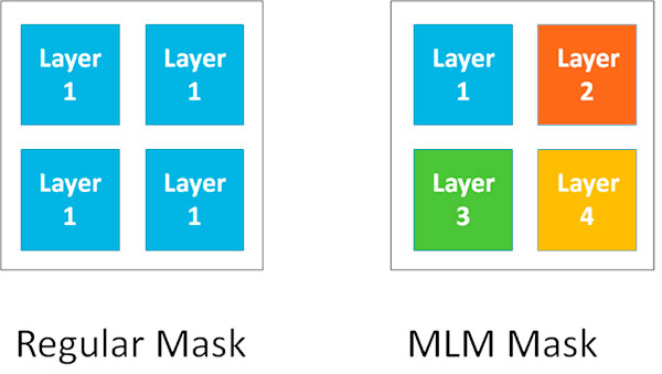
MLM Masks
Another approach to mask reduction is Multi-Level Masks (MLM). In this approach, the area of the reticle is divided up into 4 areas. A specific mask layer is put into each section, resulting in an overall mask cost reduction of 75%. Actually, the cost savings are less, since different mask layers have different resolutions, and therefore different costs.
The disadvantage is that since the mask area for a given layer has been reduced by 75%, it takes 4 times longer to expose a wafer. And that translates into a higher wafer cost. It also affects fab capacity, and so MLM masks may not be offered by the larger fabs.
Economically, there is a point at which the increase in wafer cost equals the cost for a production mask set. We reach this point at about 35 wafers. With a medium sized circuit of 5x5 mm, that translates into a 35,000 unit order. At volumes below this point, MLMs are the best approach. Above that point, a full mask set is better.
Gate Array Architectures
Our 180 nm basic process has 24 mask layers. By using a gate array architecture for the digital logic and analog circuitry, it is possible to program a gate array with 3 to 4 metal layers, or 6 to 8 masks, counting the vias. Using an existing gate array reduces the mask cost by 66% to 75%. This puts the cost of the programming layers for a gate array on par with the costs for a shuttle run.
Another way of looking at this is to note that the costs of a shuttle run followed by a full mask set is comparable to the costs of a full mask set, followed by a programming layer revision, if necessary. And this approach can be much faster than a shuttle run. A shuttle run can take four months, while a gate array can be started before the final design is done, allowing wafers to be held at the first programming layer. So a gate array cycle can be 3 to 4 weeks, instead of 4 months.
In many cases, Tekmos may already have base wafers. For example, we have a base array with multiple block RAMs, clock modules, 256 pins, and a SERDES. If the customer design fits in this base, then the programming layers are the only masks that have to be purchased, resulting in a substantially lower NRE.
Design Merges
An approach for a customer with multiple designs is to merge the designs into a single circuit, and implement that as an ASIC. Each design can be activated as a bond option during assembly, and operate as a stand-alone chip. This approach shares the mask costs over several design, without the production die cost penalties associated with a shuttle run.
Design merges are complicated. When they share pins, you have to address potential conflicts between output strengths and input levels. Supply pins add a further complication. And it is essential that the circuit that is disabled not draw power when the other design is enabled. We joke that every semiconductor company has tried design merges, and every one of them has sworn to never do it again. But in our case, we have solved the problems, and regularly use design merges.
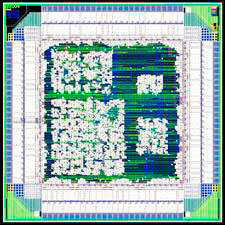
This drawing shows a merge of 4 designs on a single die.
Request for Product Information
Masks are expensive. But there are creative design and layout approaches that can substantially reduce them. Click this button to find out how Tekmos can reduce your NRE costs:
Microprocessors
Other Products
Main Office
Tekmos, Inc.
14121 Highway 290 West
Building #15
Austin, TX 78737
Phone: (512) 342-9871