
Stacked Die
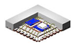 Stacked die is an assembly technique where two or more die are stacked and bonded in a single package. This was originally developed as a method of putting two memory chips in a single package to double the memory density. The term “stacked die” is often used whether the second die is on top of the first die or next to it. Today, the technology has progressed so that many die can be stacked, with the total limited by the package thickness.
Tekmos views stacked die as a way to combine different technologies into the same package. We have been using this approach for over a decade to combine flash memories with ASICs to create microcontrollers and specialty memories. Now, this is the basis for our Unify - ASICs for Your SiP market.
With Unify, we combine a processor with our mixed signal ASIC and perhaps a third chip containing a memory or special function into a single package. This creates a single chip solution for those applications where space, power, and cost is important.
But why not just make a single chip with all of these features?
Mixing Technologies
Semiconductor processing has split into various branches that have been optimized for different product types. One of the first splits occurred with DRAMs, whose need for capacitors required special processing. Another split occurred as Flash memories required a process providing floating gates and specialized gate oxides. And advanced processors left the basic digital and analog markets behind with their needs for high speed and high gate count.
These processes are incompatible, which requires systems to be composed out of multiple die. They can be packaged individually and mounted on a circuit board, or they can be stacked together in a single package.
Interconnect
Stacking the separate die in a package produces interconnect problems. The assembly industry is trying to address this with a combination of glass wafers and TSV (Thru Silicon Vias).
Tekmos addresses this through adjusting the pinout of our ASIC. Then we stack another die on our chip, and use our ASIC to serve as the means of interconnect.
When we need a triple stack, we can use a flip chip approach to put one die onto our ASIC, and mount the third die on the back of the flipped chip.
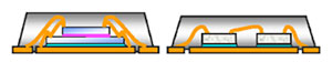
If there is room, it is possible to create two die stacks. Typically, this would be used to include MEMs into the design.
Testing
Testing is more difficult in a complex system, especially if one of the die is hidden with no external connections. Tekmos address this by installing test modes in our design that enable the complete testing of each component in the stacked die package.
Request for Product Information
To request information on our Stacked Die click this button:
Microprocessors
Other Products
Main Office
Tekmos, Inc.
14121 Highway 290 West
Building #15
Austin, TX 78737
Phone: (512) 342-9871