
Tekmos Talks Newsletters
A newsletter for the semiconductor industry
Tekmos Talks 2021
|
|
||
| A Newsletter for the Semiconductor Industry | ||
| June 2021 | ||
| Welcome to Tekmos Talks. This month Lynn will talk the Hunt for SCR and Inside Tekmos Teams. | ||
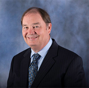
| From the Desk of the President, Lynn Reed | ||
|
The Hunt for SCR This is a story of how we inadvertently created an SCR while using externally sourced physical IP, and how we discovered and fixed it. Background SCR stands for Silicon Controlled Rectifier. It consists of a PNPN structure, as contrasted to bipolar transistors with a NPN or PNP structure. Once a SCR has been triggered, it remains on until an external event stops the current. Almost all CMOS circuits have parasitic SCRs everywhere in the layout. A P diffusion in the N-Well, in the P-substrate, next to a N diffusion creates a parasitic SCR. The key is to avoid triggering the SCR. This is done by adding substrate contacts to the wells to prevent voltage drops that might allow a P or N diffusion from becoming forward biased. Particular attention has to be paid to N-Wells that are connected to a supply other than Vdd. Our Circuit We designed a specialty 5-volt memory consisting of an 8K byte RAM, and a shadow EEPROM that could write or recall all 64K bits in a single operation. The design contained EEPROM IP, and an analog section that generated timing and monitored the power supply. The EEPROM IP consisted of a bit cell, and a driver cell that switched power supplies from 5 volts to a charge pump to program the EEPROM. In our application, we wanted to drive 256 cells instead of the recommended 16 bits. We ran spice, and the switching waveforms looked satisfactory. The First Pass SCR Problem The first silicon came back, and whenever the supply exceeded about 5 volts, and we did a store function, the part latched up, drawing amperes of current. Below 5 volts the part worked as expected. We reviewed the layout and DRCs, but did not find anything wrong. So, we sent the part to a failure analysis lab, and asked them to identify where the current was flowing. They came back with thermal images showing current flow in the analog portion of the chip. We didn’t see anything wrong in that area, but we massively increased the number of substrate contacts to minimize the possibility of any forward biased N-Wells in the area. We also added a number of test points that allowed us to disable and bypass portions of the analog circuitry in case we still had a problem. The Second Pass Problem We made new silicon, which still exhibited SCR characteristics. And our bypass circuits had no effect. We went back to the failure analysis lab with special hardware that allowed us to trigger the SCR. This time, thermal imaging showed a portion of the RAM array in SCR mode. The initial failure analysis had taken images of the chip when it was not in SCR mode, and had identified the small currents that were present in the opamps and bias circuitry in our analog design. This led to the mistaken assumption that the SCR was in the analog area. We analyzed the area indicated in the thermal imaging, and again, found nothing wrong with the layout. We analyzed the design, and discovered that an illegal condition of storing and recalling at the same time could result in a high current condition. Calculations showed that the currents caused by this condition were in the ampere level, and might be mistaken for an SCR. Could this be the problem that we were attributing to an SCR? We thought so, and redesigned the controller to ensure that a store and a recall could never occur at the same time. The Third Pass Problem We made new silicon, and it still had an SCR. So, we returned to the failure analysis lab. We used FIB (Focused Ion Beam technology) to put pads on every node we could think of for microprobing. And every signal looked fine until we did a store command, after which the part latched up. While we were at the lab, we took multiple thermal images. While doing this, we noticed that the area that had an SCR was related to the current limit we had on the power supply. With very low current limits on the supply (10 mA), we saw the SCR move from the RAM to one of the IP cells we were using to control the EEPROM. Still, even in the IP cell, the layout was correct, and there was no reason for an SCR to be there. Since we had seen the SCR area move once, we assumed that it could have moved twice, and began studying the IP to determine if there was the possibility of an initial SCR elsewhere. Our theory was that since an SCR causes local distortion of the power busses, we could have an initial SCR, which triggered another, stronger SCR, which in turn shut off the weaker initial SCR. Then, this second SCR triggered a stronger SCR in our RAM area. And the RAM SCR was strong enough to turn off the second SCR. This is a complicated theory, but if true, it would explain what we were seeing. To fix the problem, we had to identify the initial SCR. We were never able to image the initial SCR, but we assumed that it had to be close to the second SCR which we had imaged. We studied the layout, and identified an N-Well in the IP that switched the EEPROM programming voltage from Vdd to the charge pump output, and back again. After a lot of spice runs, we decided that we could create a forward bias on N-Well if the load capacitance was large enough. And we have a very large load capacitance. Much larger than the IP was designed for. We had used the same IP to control an 8-bit register that we used to calibrate timing. In order to prove that switching could cause an SCR, we ran the IP at both elevated temperature and elevated voltages. And we were able to trigger an SCR. This confirmed that we knew how the SCR was being triggered. The Fix The IP was used to drive a row of 256 EEPROM cells. Since we already had wafers at contact, we didn’t want to make any changes to previous layers. We realized that we could modify the IP in metal and working with two adjacent IP cells, make one IP drive 512 bits, and the other drive just the N-Wells used to switch the supplies. Still, we didn’t want to wait on new silicon to prove we had fixed it. So, we developed a plan to disable all of the RAM except for two rows, and use FIB to implement the fix there. This worked, and there was no sign of an SCR, even at elevated temperatures and voltages. Epilogue We then revised our layout, and made new silicon. The fix worked perfectly. And the new parts worked over elevated temperatures and voltages with no sign of an SCR. Problem solved.
|
||
| Inside Tekmos Communication | ||
|
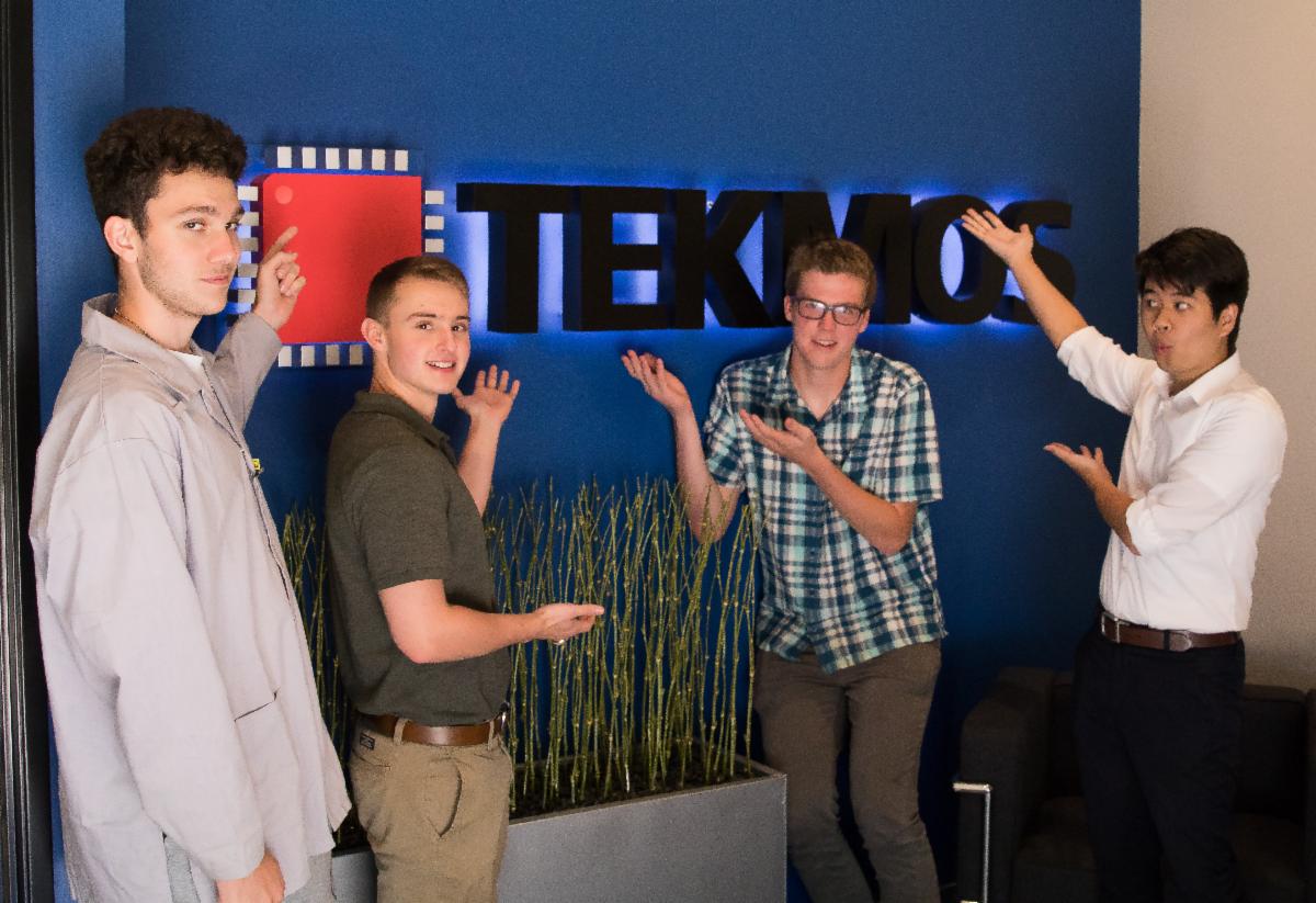
Since our move to Tekmos' new location our various Teams have started a more effective communication process using Microsoft Teams, a business communication platform that can be used from the desktop or smart phone. Every weekday morning we have a Production Focus meeting with Team members from operations, assembly, quality, test floor, customer support and accounts payable/receivable. It has become an excellent way for each of us to start our day, relay our focus for the day, to share news and information, and to ask questions and clarify between departments about orders for customers. Our Engineering Team also meets every morning to discuss the projects, share files they are working on and to update one another. Tekmos Manufacturing Production Weekly meetings have become more effective in tracking part assembly, inventory and production. Microsoft Teams is regularly used by all Tekmos Team members to speak directly to one another in face time, instant chat and along with group meets. It offers workspace chat and videoconferencing, file storage, and application integration making Tekmos communication across our departments much more efficient and a pleasant gathering space.
|
||
| Inside Tekmos | ||
|
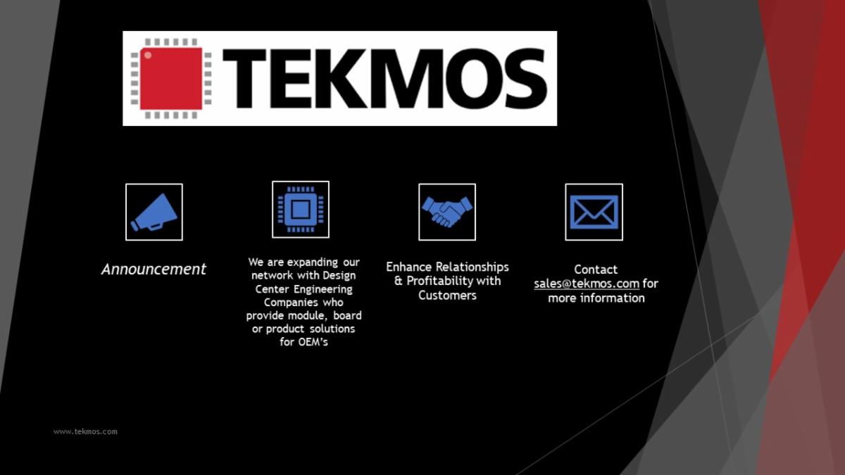
Tekmos Expands Partnerships with Design Engineering Companies
We have expanded our network with design center engineering companies, who provide the module, board or product solutions for OEMs. Our value is in providing an ASIC solution and a multi chip packaging solution, which can include chips with mixed technologies into a final device that is fully tested. If you work with ASIC companies and you have a need to build something unique or to combine multiple die into single package to save space, our program is designed to work as a partnership. Feel free to contact Tekmos about the value Tekmos offers to enhance your relationship and profitability with customers.
|
||
| Thank You for Reading Tekmos Talks | ||
|
Thank you for reading Tekmos Talks and helping us celebrate 20 plus years. Sincerely, Lynn Reed, President
|
||
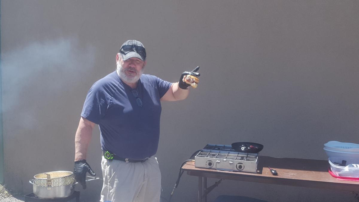 Phil Buck, Chief Cook & Organizer
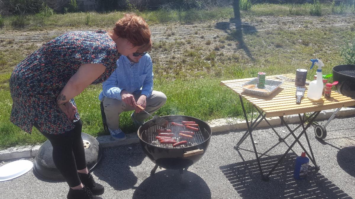 Cameron assists in cooking with Carole overseeing.
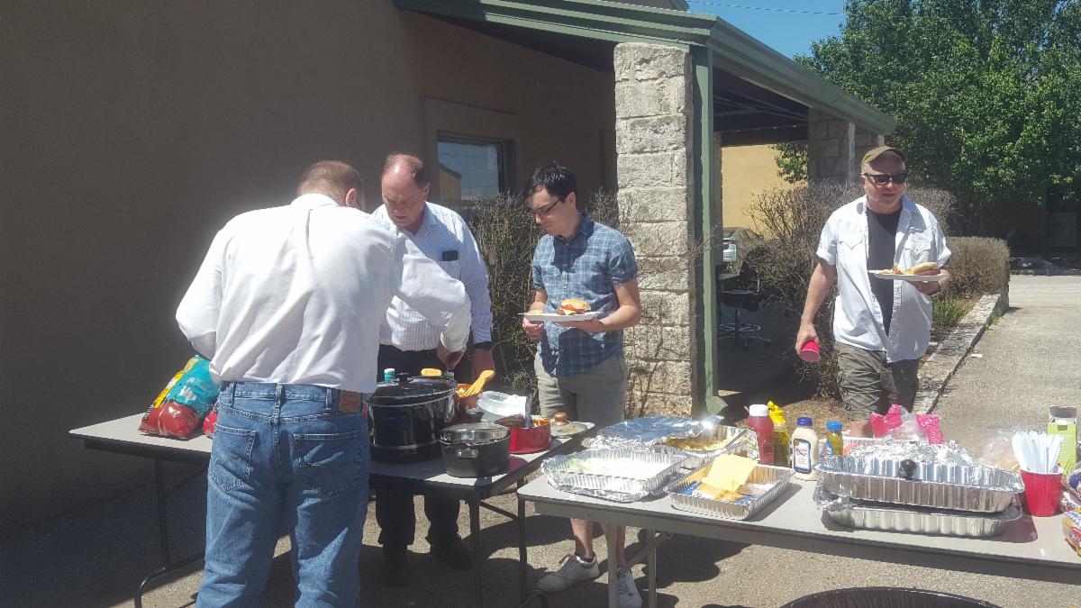
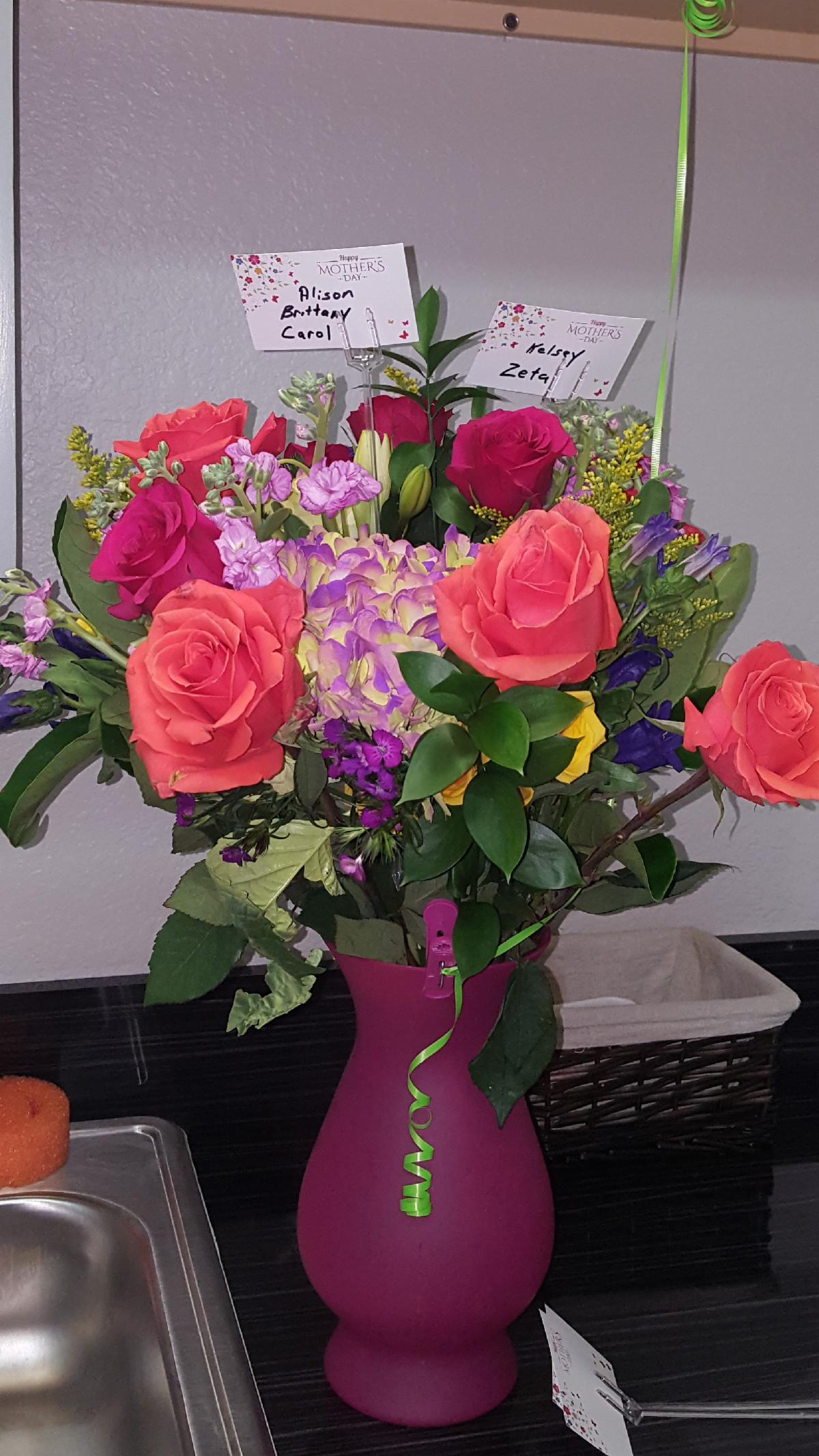 Phil also honored the mothers of Tekmos with a lovely bouquet of flowers.
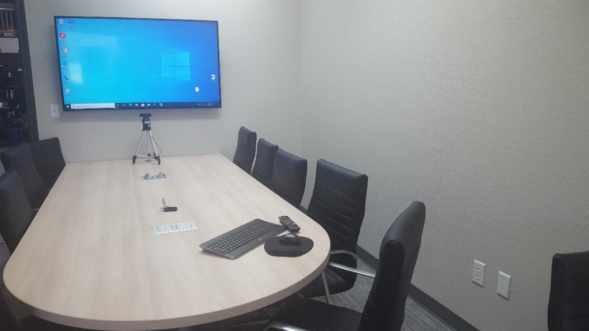 Conference Room
 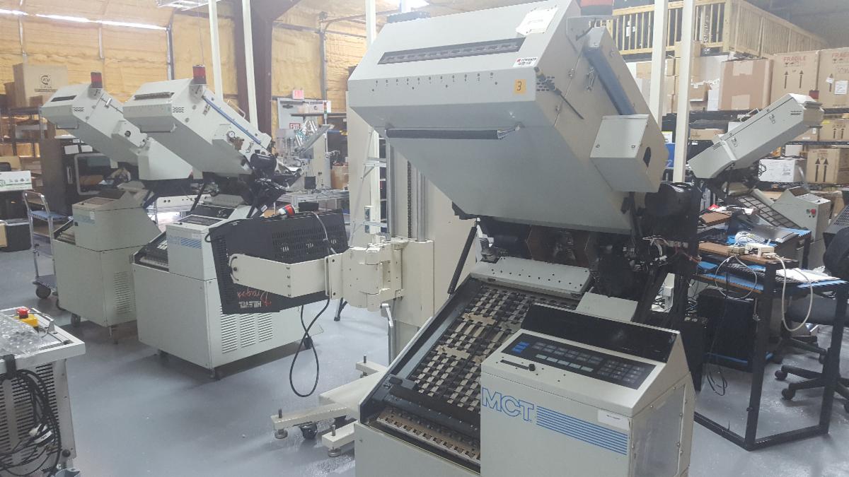 Test Floor
 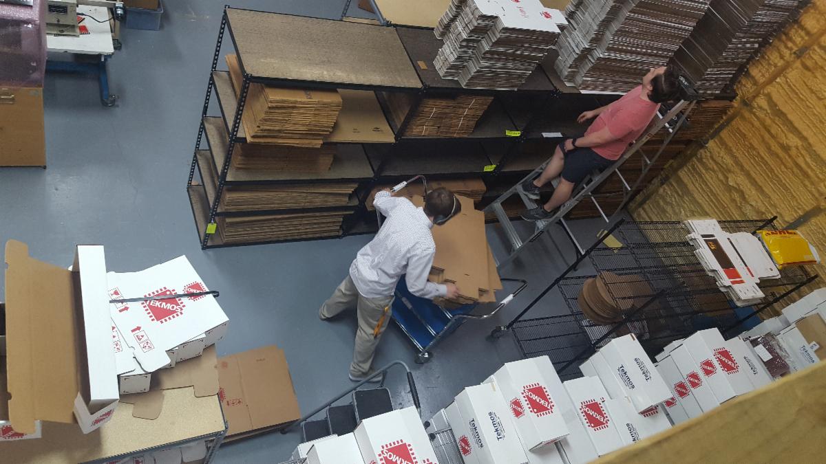 Shipping Department
 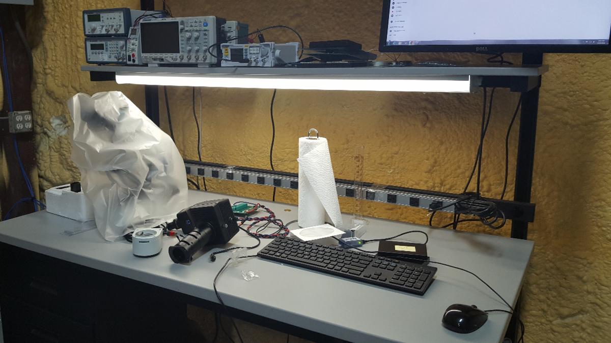 Engineering Lab
 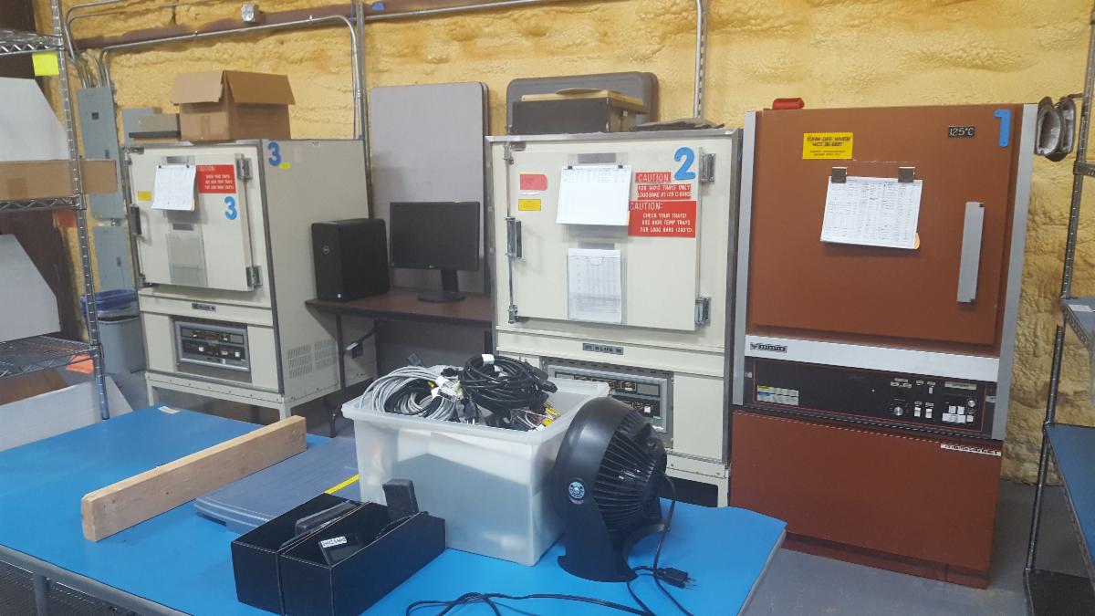 Test Ovens
 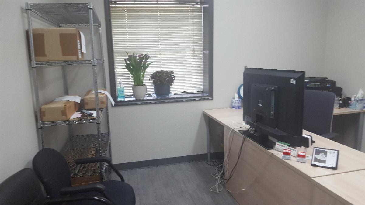 Production Office
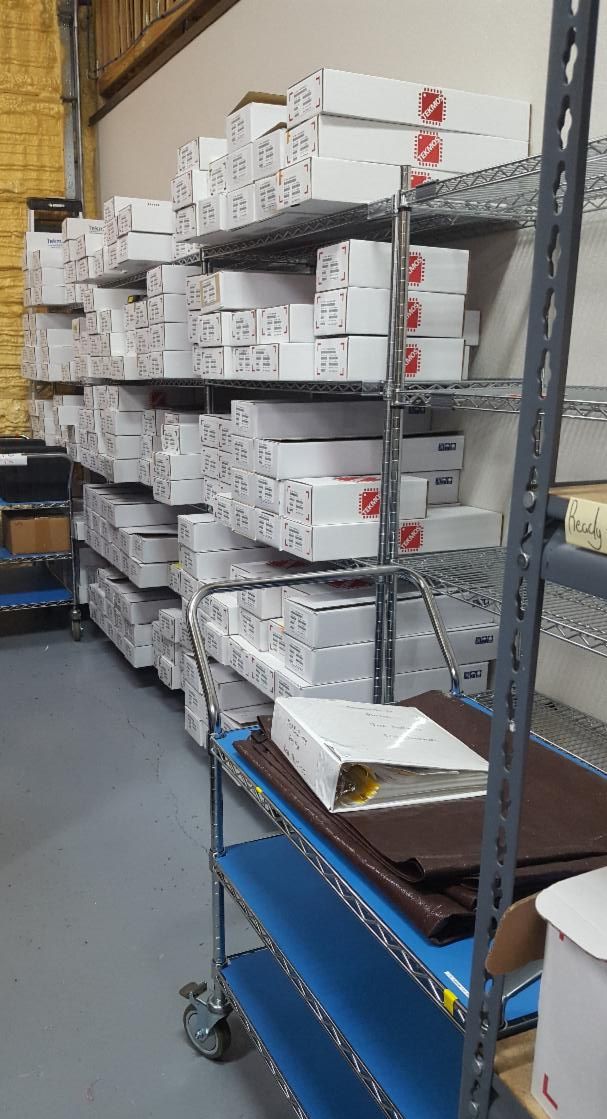 Tekmos Finished Projects
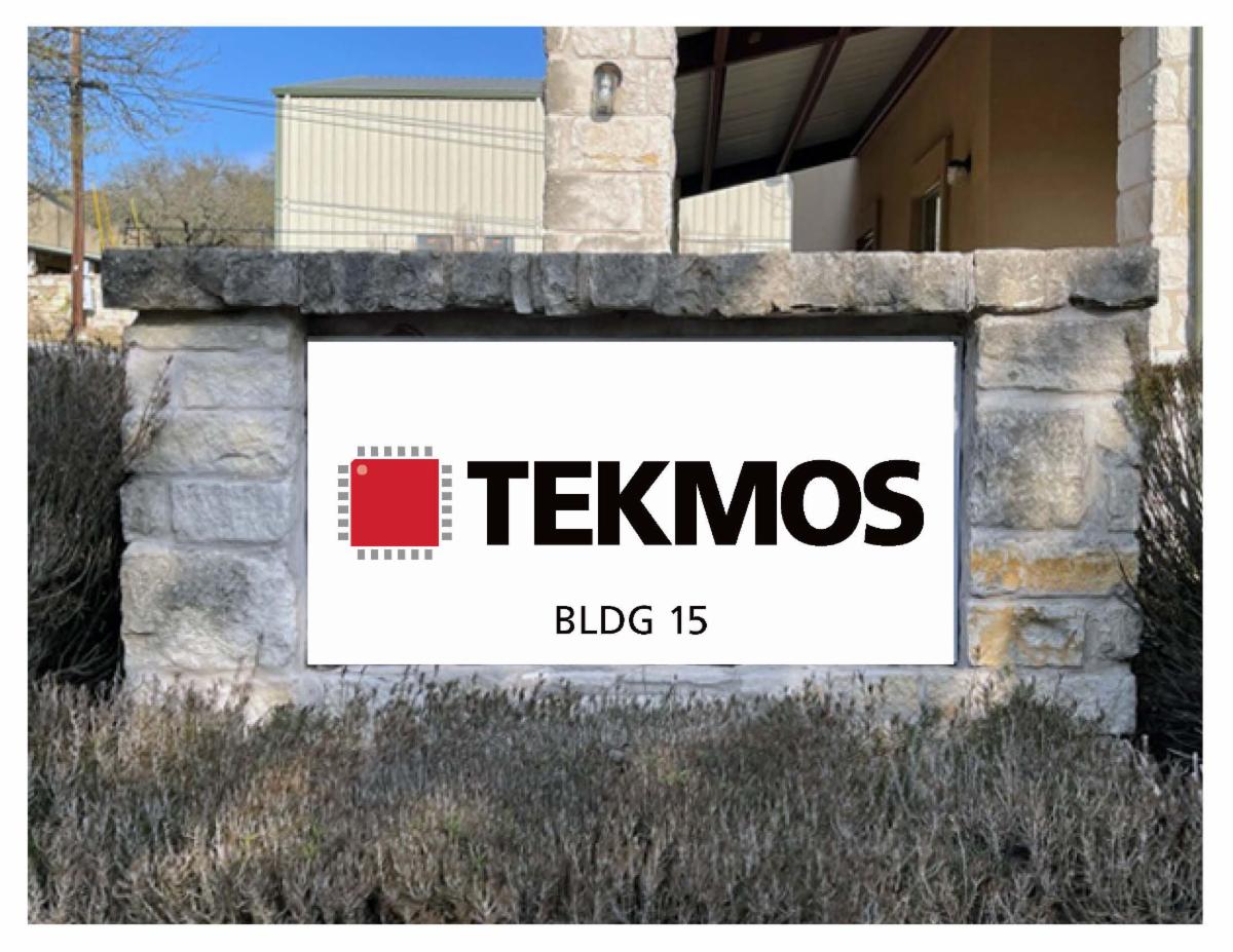 14121 Highway 290 West, Building 15 Austin, TX 78737
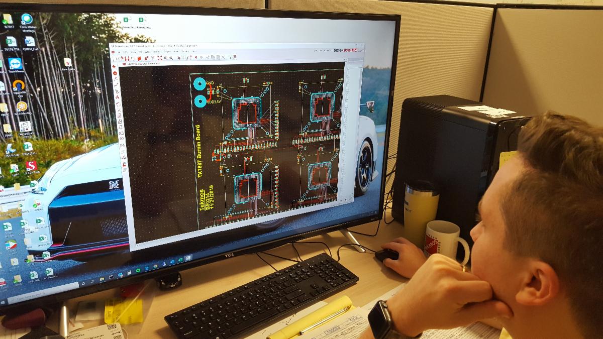
 Kelsey Casto, and husband, Cy are happy to announce the birth of daughter, Cypress 5lb.7 oz., 18 inches
 The new facilities are mainly for manufacturing. Testing, baking, tape and reeling, and shipping must be done on-site. On the other hand, professionals will work remotely, reducing the need for on-site offices and cubes.
 Being effective in the workplace means so much more now. The COVID-19 pandemic has changed the work paradigm permanently. Workers around the world have had to adjust to that change wearing masks, social distancing, communicating specifically, succinctly, and often, to working remote part, or all the time, adding stress.
 As more of us work remote, fresh ideas are needed to keep the work Team connected.
 Do people love remote work? For most, including at Tekmos, they do, and it’s mainly the flexibility. Travel and commute are reduced including the cost of both. There is a reduction of distractions. The ability to travel and live anywhere, including outside of major cities offers workers the ability to be closer to family. A big plus is often an increase in productivity.
 What brought you to Tekmos?
Tekmos Talks
Main Office
Tekmos, Inc.
14121 Highway 290 West
Building #15
Austin, TX 78737
Phone: (512) 342-9871